
CanSemi IPO: Silicon Photonics and Fab Hiring | SunTzu China
CanSemi priced its ChiNext IPO at RMB 12.01, lifting capacity from 63,000 to 120,000 wafers a month. Silicon photonics engineers are scarce in South China.

On September 24, CanSemi Technology (301660.SZ) opened its ChiNext subscription at RMB 12.01 per share, with an initial public offering of 513 million shares, or 17.81 per cent of the post-issuance share capital. The allotment announcement released on the evening of September 27 showed 14.44 million valid online subscriber accounts and 423.38 billion shares effectively subscribed. After the clawback mechanism was triggered, the final online tranche came to 179 million shares, putting the online allotment ratio at 0.0424 per cent against an effective subscription multiple of 2,359.68 times. The company, based in Huangpu district of Guangzhou, is known across the industry as Guangzhou's first chip maker: the first 12-inch wafer fabrication plant in Guangdong province to reach mass production under local ownership.
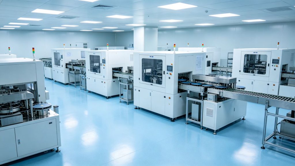
For the talent market, the signal in this IPO sits in the capacity table rather than the share price. The prospectus shows two existing 12-inch fabs with a combined planned capacity of 80,000 wafers per month, of which 63,000 wafers per month had been realised by the end of 2025. A third fab with a planned capacity of 40,000 wafers per month is under construction; once complete, total capacity will reach 120,000 wafers per month. Behind that near doubling sits a multi-year hiring list, and one role category on the list has almost no existing pool in South China: silicon photonics.
1. The Capacity Table Is the Hiring Table
Founded in 2017, CanSemi brought its first production line into mass production in 2019, ending the period in which Guangdong had no local 12-inch wafer fab in volume manufacturing. Over nine years, the province's shortage of chips and cores has been rewritten into the starting point of a one-core, two-pole layout: Guangzhou's integrated circuit industry is anchored in Huangpu, with Nansha and Zengcheng as the two poles, and CanSemi, XinYueNeng and Zengxin Technology all in production.
The pace of capacity ramp sets the pace of hiring. Annual capacity ran at 449,500 wafers in 2023, 478,000 in 2024 and 614,800 in 2025, with utilisation rising to 96.38 per cent in 2025. Revenue over the same three years was RMB 1.044 billion, RMB 1.681 billion and RMB 2.582 billion, a compound annual growth rate of 57.30 per cent. Utilisation close to full load means the next leg of growth has to come from new lines; squeezing more out of the existing fabs has limited room left. That is the direct reason the fourth phase was launched, and it also marks the point where hiring moves from backfilling to building an organisation.
A linear extrapolation on current productivity makes the scale visible. With 1,943 employees against 63,000 wafers per month of realised capacity, the company runs at roughly 307 people per 10,000 wafers of monthly capacity. If total capacity reaches 120,000 wafers per month at unchanged productivity, headcount approaches 3,700, a net addition of about 1,700. That figure needs to be discounted: automation gains, yield improvements and a higher outsourcing ratio will all reduce actual demand. Even so, it establishes the order of magnitude. This is organisation-building recruitment, far larger than a backfill exercise of a few dozen roles.
| Item | 2023 | 2024 | 2025 | H1 2026 |
|---|---|---|---|---|
| Annual capacity (k wafers) | 449.5 | 478.0 | 614.8 | Not disclosed |
| Realised monthly capacity (k wafers/month) | Not disclosed | Not disclosed | 63.0 | Not disclosed |
| Revenue (RMB bn) | 1.044 | 1.681 | 2.582 | 1.777 (+68.76% YoY) |
| Net profit attributable to parent (RMB bn) | -1.917 | -2.253 | -2.346 | -1.052 |
| Main business gross margin | -114.90% | -71.00% | -58.24% | Not disclosed |
| Capacity utilisation | Not disclosed | Not disclosed | 96.38% | Not disclosed |
| Total employees | Not disclosed | Not disclosed | 1,943 | Not disclosed |
Depreciation is the other set of numbers HR should read closely. Over the reporting period, depreciation of machinery and equipment totalled RMB 5.523 billion against revenue of RMB 5.307 billion. Depreciation exceeded revenue, which is the typical early-stage profile of a capital-intensive fab and the main source of the losses. Government grants recognised in profit or loss over 2023 to 2025 came to about RMB 1.203 billion. The company expects to reach break-even on a consolidated basis no earlier than 2029.
The implication for pay strategy is direct. While depreciation pressure remains undigested and gross margin is still negative, broad increases in cash compensation lack a financial basis. The company has taken a different route, moving retention cost forward into the capital structure, which is set out in section four.
2. Silicon Photonics: A Role Category That Barely Existed in South China
CanSemi's process platforms split into seven, six of which sit on mature ground. The MS platform serves fingerprint sensors, LED display drivers and power management. The high-voltage HV platform fits LCD panel drivers and electronic shelf label drivers. The CIS platform serves smartphone and security imaging sensors. The BCD platform covers battery management and power management. The eNVM platform supplies embedded memory for consumer and industrial MCUs. The MOSFET and IGBT platforms address new energy vehicles, photovoltaics and industrial variable frequency drives. All six have established supply pools in China; matching candidates can be found in the Yangtze River Delta, the Beijing-Tianjin-Hebei region and Chengdu-Chongqing.
The seventh is the variable. CanSemi launched a 12-inch 90nm silicon photonics platform at the end of 2024. According to Frost & Sullivan data, as of the end of April 2026 it was the only company in mainland China with large-scale mass production capability for 12-inch silicon photonics wafers, with products covering 400G, 800G and 1.6T high-speed pluggable optical module applications and broadly in line with international leading standards. The company is also developing near-package optics (NPO) processes and moving 3.2T NPO products into production.
The question then lands on people: where are they? Listings on public recruitment platforms show silicon photonics engineer roles concentrated in Pudong in Shanghai, Nanshan in Shenzhen, Xihu in Hangzhou and Optics Valley in Wuhan, with almost none in Guangzhou. A senior silicon photonics chip design engineer role in Pudong lists at RMB 60,000 to 90,000 per month across 15 months, requires a master's degree or above and more than seven years of industry experience in optoelectronic devices, and covers passive and active device design, waveguide layout and simulation, and device testing and characterisation. The posting explicitly prioritises engineers with volume production experience on 400G, 800G or 1.6T products, and states that both pay and share incentives are negotiable. A comparable role in Nanshan, Shenzhen lists at RMB 70,000 to 100,000 per month across 15 months with three years of experience required. A silicon photonics design role in Xihu, Hangzhou lists at RMB 60,000 to 90,000 per month across 14 months, requires eight years of forward design experience on silicon-on-insulator photonic integrated circuits, and names Lumerical FDTD/MODE/EM and KLayout in the tool chain requirements.
Pay is one filter; capability verification is another. Silicon photonics differs from digital chip design in the certainty of tape-out verification. Digital design can rely on a mature PDK to keep the gap between simulation and silicon within an acceptable range. Silicon photonics depends heavily on the process stability of a specific foundry's PDK, and significant gaps between simulated and measured results are common. The effective interview questions for this role are therefore not which devices have you built, but which foundry's PDK did you use, which version, what range did simulation-to-silicon deviation usually fall in, and how many MPW tape-out cycles have you been through. Candidates who can answer all four with specific numbers are scarce anywhere in the country.
For companies in South China, the standard local-first, external-supplement hiring configuration does not work for silicon photonics. There are three workable paths. First, bring in a core group from established silicon photonics teams in Shanghai, Shenzhen or Wuhan, trading project authority and equity against the cost of relocation. Second, co-develop talent with the foundry side so that process adaptation capability accumulates in people. Third, accept a division of labour in which front-end device design sits elsewhere and process integration and volume ramp sit in Guangzhou. Each path implies a different compensation package, and choosing the wrong one pushes the hiring cycle beyond twelve months.
3. A Portrait of 1,943 People
As of December 31, 2025, the company employed 1,943 people. Staff with a master's degree or above accounted for 20.48 per cent, more than 60 per cent had three or more years of semiconductor industry experience, and 343 worked in R&D. The company also states that its technical and management specialists come from around the world, that the core management team carries more than twenty years of industry experience, and that a reasonable talent pipeline has been built.
Read together, these numbers establish what matters most. R&D staff at about 17.65 per cent is not high for a foundry, because the bulk of foundry talent does not sit in a laboratory; it sits on the production line. A little over one in five holding a master's degree or above means the core of the workforce is made up of process, equipment and manufacturing staff with bachelor's degrees. With more than 60 per cent holding three years of industry experience, this is a workforce that has to be recruited from the existing market; campus hiring alone is too slow to build it.
| Indicator (as of December 31, 2025) | Value | What it means for hiring |
|---|---|---|
| Total headcount | 1,943 | At roughly 307 people per 10,000 wafers of monthly capacity, 120,000 wafers/month implies about 3,700 people (modelled; actual figure falls with automation and outsourcing) |
| R& D staff | 343 (about 17.65%) | R& D is not the main demand; process integration and volume manufacturing engineering are |
| Master's degree or above | 20.48% | Core demand sits with bachelor's-level process and equipment engineers who have line experience |
| Three or more years of semiconductor experience | Above 60% | Hire experienced staff from the existing market; campus hiring is a supplementary channel |
| Equity incentives for core staff | Implemented | Retention tooling is already in place; cash is not the only negotiating lever |
| Customer coverage | Over 200 in total, nearly 40 listed companies domestic and overseas | Requires customer engineering and automotive-grade quality talent (IATF 16949, VDA6.3) |
| Granted patents | 712, including 343 invention patents | Process development roles need patent drafting and technical documentation capability |
Broken down by process platform, demand is unevenly distributed. BCD and power device platforms (MOSFET, IGBT) serve battery management, power management, new energy vehicles, photovoltaics and industrial drives; power device engineers of this kind exist in both the Yangtze River Delta and the Pearl River Delta, so hiring difficulty is moderate. The CIS platform serves mobile and security imaging sensors, with the pool concentrated in companies that run CIS lines. eNVM and embedded memory for MCUs are relatively niche and domestic supply is limited. The HV platform is tied to display drivers and its supply moves with the panel cycle. Only silicon photonics is genuinely scarce.
The quality function deserves early attention as well. The company holds ISO 9001, ISO 14001, ISO 45001 and ISO 50001 certifications, has passed IATF 16949 for automotive production lines, and has built a full lifecycle quality management system for automotive-grade chips against the VDA6.3 process audit standard of the German Association of the Automotive Industry. Running that system requires people who understand both the production line and the audit framework, and that combination is also in short supply locally.
4. Retaining Talent Through a Loss-Making Phase
Three consecutive years of losses are an unavoidable premise. Net profit attributable to the parent company was RMB -1.917 billion, RMB -2.253 billion and RMB -2.346 billion over 2023 to 2025, a cumulative total of about RMB 6.516 billion; on a net profit basis the cumulative figure is about RMB 6.734 billion. Undistributed profit stood at RMB -10.081 billion at the end of 2025. The company expects consolidated break-even no earlier than 2029.
Against that financial structure, CanSemi's retention design has two observable parts. The first is conventional: the company discloses that it has implemented an equity incentive plan for core staff to improve the stability of the core team and support innovation. The second is the one HR should study. In the strategic placement for this IPO, two dedicated asset management plans set up for CanSemi senior management and core employees were allocated 16.9011 million shares and 825,300 shares, worth RMB 203 million and RMB 9.912 million respectively. In other words, core employees were given a direct holding channel at the listing stage, tying personal upside to post-listing market value.
That design has a clear time boundary. Dedicated asset management plans usually carry a lock-up period, and the retention effect is strongest inside it. Once the lock-up ends while the company is still loss-making, pressure from both share price performance and cash compensation arrives at the same time. With 2029 as the expected break-even point, 2027 to 2029 is the high-risk window for attrition among core staff. The lesson for HR is that a single equity grant is not enough. A second instrument needs to be launched twelve to eighteen months before the lock-up expires, whether that is a new grant tranche or a shift of cash compensation onto a schedule linked to profitability milestones.
The implication for external hiring is equally direct. When equity is the main negotiating lever, three things have to be stated clearly: vesting conditions, lock-up length, and the timetable from loss to profit. An offer that is vague on these three points will be heavily discounted in the candidate's own valuation.
Designing a compensation package at a pre-profit technology company is largely about converting uncertain equity into a certainty the candidate can evaluate. A workable method is to translate the equity into a banded annual value, place it alongside the cash component in the offer, and state when the next valuation review will happen. What candidates resist is not risk itself; it is not knowing how large the risk is.
5. Geography: What Guangzhou Offers, and What Policy Adds
The semiconductor talent supply structure in South China has a distinctive shape: strong in design, weak in manufacturing. Shenzhen hosts a large number of chip design companies and chip design talent, Dongguan has a complete packaging and testing industry, and Foshan and Zhuhai each have positions in semiconductor materials, but 12-inch wafer manufacturing was a long-standing blank before CanSemi. That means the process, equipment, yield and facility talent CanSemi needs has almost no local counterpart in South China, and the main sources are the Yangtze River Delta, Beijing-Tianjin-Hebei, and returnees with experience at overseas fabs.
Policy is working on that gap. The twelve measures in the Guangzhou municipal policy on promoting high-quality development of the integrated circuit industry across the full chain during the 15th Five-Year Plan period, issued for consultation by the city's industry and information technology department, concentrate resources on high-end chip R&D, 12-inch wafer manufacturing, advanced packaging and testing, and key materials and equipment. Companies that carry out tape-outs of self-developed chips at 28nm and below, or of chips with significant competitive advantage, receive subsidies of up to 50 per cent of tape-out cost, capped at RMB 5 million per company per year. Particularly large projects may be supported through a subsidy-to-equity conversion, with support not exceeding 20 per cent of new equipment purchase value and an equity stake of no more than 30 per cent in the project company.
The talent-side policies are more specific. In Guangzhou Development Zone and Huangpu district, qualifying full-time doctoral degree holders (or those with senior professional titles or chief technician status), master's degree holders (or those with associate senior titles or senior technician status), and bachelor's degree holders (or technicians) receive one-off housing vouchers of RMB 250,000, RMB 150,000 and RMB 100,000 respectively. After stable employment, they can receive a monthly rental subsidy of RMB 800 to RMB 1,500 for 24 months, a home purchase subsidy of up to RMB 300,000, and outstanding scientific and technological talent can receive home purchase subsidies of up to RMB 3 million. Postdoctoral researchers can receive up to RMB 800,000 in research funding and living allowances during their tenure. Huangpu district also ran a recruitment mission to Shanghai, Jiangsu, Zhejiang and Anhui from September 16 to 21, 2026, holding dedicated sessions at Zhejiang University and the University of Science and Technology of China. Guangzhou chip talent supply is thin locally, and the district government is already going directly to Yangtze Delta universities to find people.
The practical value for HR is that these policies belong in the offer. For a senior process engineer brought in from Shanghai, a RMB 250,000 doctoral housing voucher or RMB 150,000 master's housing voucher in Huangpu, plus a rental subsidy of up to RMB 1,500 a month for 24 months, converts into a substantial cash equivalent, enough to offset part of the cost of relocating across regions. Quoting the policy package and the salary package as a combined number is currently the most overlooked and cheapest source of competitiveness for South China employers.
6. Three Recommendations for HR
First, split roles by process platform rather than recruiting against a generic semiconductor engineer profile. The seven platforms demand very different capabilities: MS and HV lean towards display drivers, BCD and power towards power management and automotive, CIS towards imaging sensors, eNVM towards embedded memory, and SiPho towards optoelectronics. Under the same process engineer title, candidate sources, pay benchmarks and hiring cycles differ completely across those seven lines. Splitting job descriptions by platform is the precondition for compressing a six-month cycle into three.
Second, price silicon photonics roles separately and accept both relocation and a division of labour. There is no local pool, and local-only hiring is an invalid path. A three-tier compensation structure works better: price front-end device design roles against Shanghai and Shenzhen market rates and accept that the role may sit elsewhere or work remotely; place process integration and volume ramp roles in Guangzhou, priced on the local manufacturing scale with equity and project bonuses attached; relax degree and tenure requirements for test and characterisation roles and instead test hands-on experience with tools such as Lumerical and KLayout.
Third, count government talent policy in the total package and write it into the offer. Housing vouchers, rental subsidies, home purchase subsidies and postdoctoral funding in Huangpu convert into more appeal for a relocating candidate than an equivalent amount of cash salary, because the former arrives as one large lump and the latter is spread thinly across monthly payments. Listing a policy component and a company component separately lets the candidate calculate the true total.
The significance of the CanSemi IPO is that semiconductor manufacturing in South China now has a reference employer for the first time. The move from 63,000 to 120,000 wafers per month will keep releasing organisation-scale demand for process, equipment, yield and facility roles. Silicon photonics is the only category that is nationally scarce, and the only one that cannot be solved from local supply. For HR, the task now is not to wait for roles to open, but to draw the talent map for all seven process platforms first, and to settle the three sourcing paths for silicon photonics in particular.
An executive search firm in China covering chip design, wafer manufacturing, packaging and testing, and equipment and materials, with practice depth in semiconductors, artificial intelligence, robotics, new energy vehicles, healthcare, cross-border e-commerce and IT and communications. For Greater Bay Area semiconductor pay benchmarking and talent mapping, get in touch with our semiconductor headhunter team.
Data note: capacity, operating and headcount figures are taken from the CanSemi prospectus, the issuance announcement for the initial public offering on the ChiNext board, and public filings between September 23 and September 27, 2026. Listed salary figures come from public recruitment platforms, represent advertised ranges rather than actual agreed pay, and change over time. Talent policy figures come from published policy documents of Guangzhou municipality and Guangzhou Development Zone / Huangpu district; eligibility is subject to the latest official wording. The headcount extrapolation is a linear calculation at current productivity and does not represent a forecast of the company's actual recruitment plan.